Volcanic Overview
Imagination’s Volcanic architecture is a programmable architecture capable of executing general purpose computations as well as rendering graphics.
As shown in the following figures, Imagination architectures provide different hardware for transferring vertex, pixel, and compute data between memory and the GPU Core, and programmable processors for performing the actual operations. Unlike the older architectures, the new generation GPUs have a dedicated path for compute tasks via the Compute Data Master (CDM), with the programmable arithmetic handled by Unified Shading Clusters (USCs).

Fig. 6 Type 3 (Volcanic) architecture and data flow overview
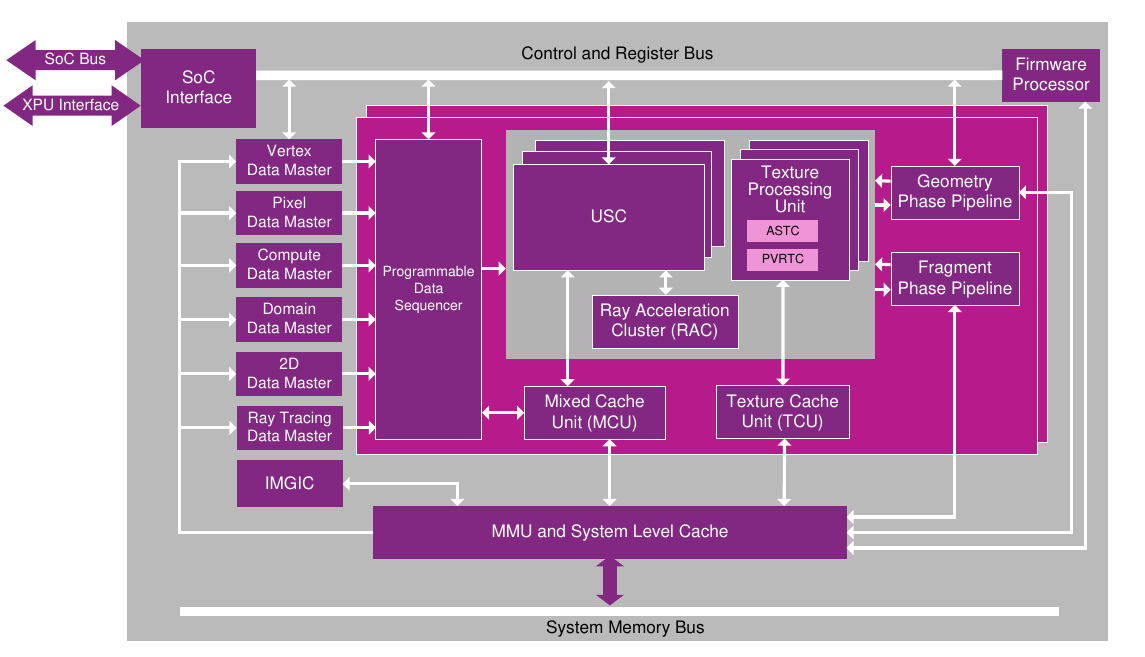
Fig. 7 Type 4 (Volcanic) architecture and data flow overview
Architecture Workflow Terminology
This section summarises the terminology used in this document to refer to the various aspects of the GPU architecture workflow.
Workload: Used to identify higher level processing for Imagination cores. For example, the 3D graphics workload, the 2D workload or the compute workload. In OpenCL, a workload is a grouping of work-items that can synchronize and share data between one another.
Data Master: A hardware unit that initiates the processing of a specific type of GPU workload, for example geometry, pixel, compute or ray tracing.
Task: Describes a collection of instances of the same type which executes the same code. Tasks can be up to 128 instances in size
Instance: A unit of USC workload processing, analogous to a hardware thread. They are executed in groups called Tasks.
Slot: A storage element within the controller of the USC or PDS (Programmable Data Sequencer)
DWORD: 32 bits.
Firmware Processor
The Firmware processor (Meta/MIPS/RISC-V) executes the GPU core firmware, which serves as the interface between the device driver and the core. The firmware processor manages scheduling and execution of workloads across the GPU core’s hardware units, while also monitoring and processing commands from the host driver. It ensures low-latency, concurrent scheduling to maximize hardware utilization. The firmware distinguishes between low-priority background (BG) tasks—such as processing new host commands, checking dependencies (fences), and preparing work—and high-priority interrupt (IRQ) tasks, which handle immediate hardware actions like starting or completing commands. The architecture supports up to 8 virtual GPUs, each with a dedicated interrupt line and thread scheduler register for independent operation.
Device Driver
The GPU core processes workloads in terms of contexts, where each context typically represents an application or task on the host system. Multiple host contexts can exist simultaneously and are mapped to corresponding GPU contexts, which manage the resources needed for processing (e.g., Render Context for graphics, Compute Context for compute tasks).
Each context can independently send commands to the firmware to initiate GPU processing. At the hardware level, these commands are handled by specialised units called Data Masters (DMs), each responsible for a specific type of workload. Compute Data Master (CDM) handles compute workloads.
Programmable Data Sequencer
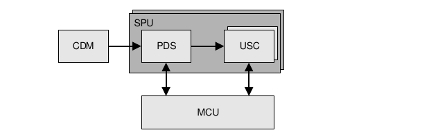
The Programmable Data Sequencer (PDS) is responsible for scheduling Unified Shading Cluster (USC) tasks and managing the resources required for those tasks across different workload types, including compute. The PDS receives requests from the Compute Data Master (CDM) and other data masters, handling each source in parallel.
Upon task completion, the PDS deallocates resources for reuse. Since the resource controller manages nearly all on-chip resources, its allocation strategy—balancing order and size of allocations for each data master—directly impacts performance and throughput. Fine-grained controls are available for resource allocation on a per data master basis, allowing the PDS to efficiently select and schedule tasks from multiple sources.
Following diagram show where these PDS units are located in the GPU architecture, and its interactions with other blocks:
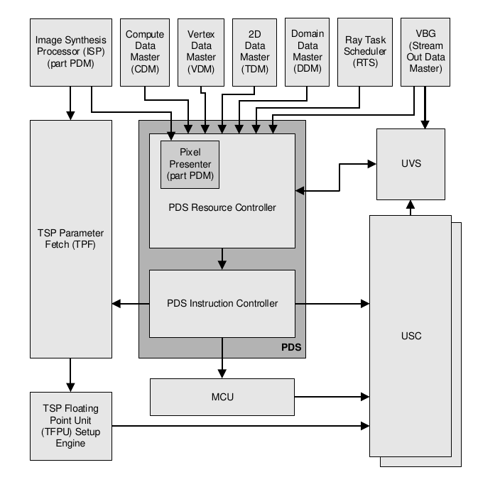
Fig. 8 Programmable Data Sequencer overview
PDS Compute Workload Programs
For compute workloads PDS runs programs to load compute kernels and data into the USC.
Unified Shading Cluster
The Unified Shading Cluster (USC) is a programmable processing unit shared by the Geometry and Fragment Processing phases of compute workloads and graphics worklads. Optimised for SIMD operations, the USC executes shaders and, and GP-GPU programs. It receives tasks from the PDS, manages their scheduling, and runs them to completion. The USC includes storage for shader execution, and outputs are sent to external modules for further processing.
An instance, or data instance represents a single iteration through a USC program. In compute workloads, an instance is a work-item. Each instance is processed by the appropriate shader or kernel. A task, is made up of a program or shader and up to 128 data instances, all executing the same shader. Some tasks may have zero valid instances and exist solely to satisfy dependency requirements.
There is space for a certain number of tasks to be managed in the USC, but only a subset of them can have resources allocated to run (occupying a slot). The number of tasks are configuration dependent.
The USC consists of multiple pipelines managed by a common control unit, which dispatches instructions to the appropriate pipeline. These pipelines are software-assisted and include dedicated hardware mechanisms to avoid data hazards during execution. An overview of the USC is illustrated below.
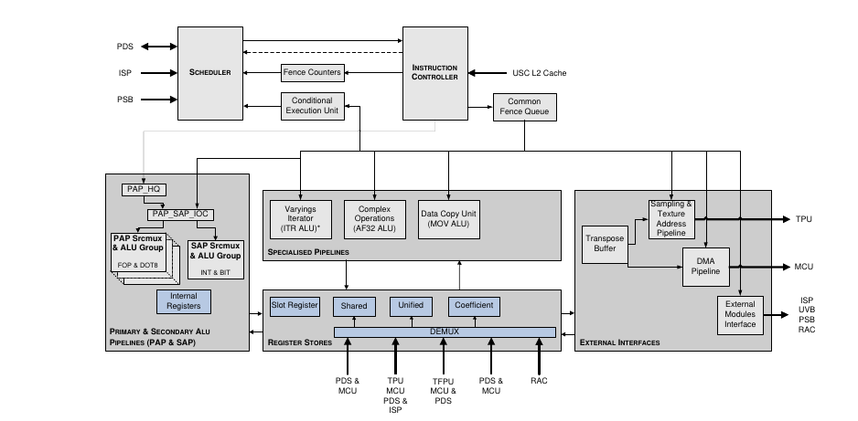
Fig. 9 Unified Shading Cluster overview
The USC processes data in units called tasks, each containing 0 to 128 valid instances. Each task is assigned to a slot in the USC Controller for execution. Tasks with no valid instances are discarded after their dependencies are resolved and are primarily used for sequencing. While task behaviour is fully programmable, there are several common usage scenarios. Compute data master tasks are multi instance tasks which operate on data in shared registers, attribute registers, and memory. For compute data master tasks, like other non-pixel shader tasks, instances are considered individually rather than in blocks of 4.
Memory Hierarchy
In the GPU core, memory addressing is managed by separate modules for the Bus Interface (BIF), caches, and the Memory Management Unit (MMU). The MMU sits between external memory and both the BIF and System Level Cache (SLC) units. The number of BIFs present depends on the number of Unified Shading Clusters (USCs) in the core.
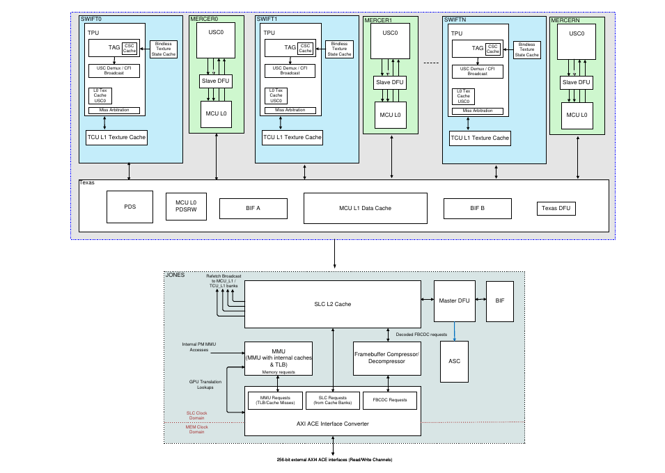
Fig. 10 Cache Hierarchy
The Bus Interface (BIF) acts as the bridge between GPU blocks requesting memory access and the memory system, i.e. the System Level Cache (SLC) and Memory Management Unit (MMU). Multiple BIF blocks share access to a single SLC, with dedicated BIFs for core GPU units. BIF modules handle interfacing with the SLC, arbitrate between multiple incoming memory requests, and reorder return data from the SLC to the requestors, as illustrated below.
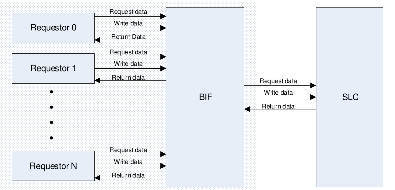
Fig. 11 BIF overview
The System Level Cache (SLC) is a high-bandwidth, multi-bank cache designed to support multiple GPU units efficiently. Each cache bank can service one instruction per clock cycle, and the cache RAM is 512 bits wide, allowing simultaneous execution of two 256-bit words when requests span both. The number of 256-bit inputs and cache banks scales with the number of Unified Shading Clusters (USCs) and Shader Processing Units (SPUs) in the core. The SLC operates fully out-of-order, reordering instructions from different requestors except when multiple requests target the same address or cacheline, in which case strict submission order is enforced. Cachelines are striped across multiple RAMs within each bank, enabling 512-bit access per cycle when possible. Each bank manages a unique subset of cachelines, and incoming addresses are distributed across banks using a hashing function to ensure even, non-overlapping allocation of the address space.
The Memory Management Unit (MMU) provides virtualized addressing by translating virtual addresses to physical addresses as requested by the System Level Cache (SLC). Virtual-to-physical address mappings are stored in translation tables in memory, which are typically set up and maintained by software. However, for certain modules or data masters, the Parameter Management (PM) unit handles memory allocation, and the MMU manages the translation tables on behalf of the PM. The MMU supports multiple memory contexts, each identified by a Context ID and 1TB virtual address space. Any GPU pipeline (Data Master) can select and use any of these active memory contexts during execution. The MMU allows different page sizes to be used, configurable via the RGX_CR_MMU_PAGE_SIZE_RANGE_* registers. These registers enable specific address ranges to be assigned particular page sizes.
Compute Workload
When a compute kernel is launched, its data is fetched from external memory and multiple concurrent kernel instances (work-items) are created. These work-items are organized into thread-groups, which are executed by the compute processing units. Each compute processing unit manages a pool of thread-groups and executes threads from one thread-group at a time. After execution, the results of the compute workload are written back to memory.
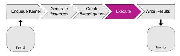
Below you can find a high level view of the compute pipeline:
The compute processing pipeline is composed of several key blocks:
Compute Data Master (CDM): Initiates compute processing by fetching control streams from external memory via the Bus Interface (BIF) and feeds compute tasks to the Programmable Data Sequencer (PDS).
Programmable Data Sequencer (PDS): Organizes work-items from the CDM into tasks suitable for execution by the Unified Shading Clusters (USC).
Unified Shading Clusters (USC): Executes the compute tasks, utilizing the Mixed Cache Unit (MCU) or Texture Processing Unit (TPU) as needed to accelerate specific operations.
USC Register Stores
The USC contains a number of different storage components used in setup of and during shader execution.
Unified Store
The Unified Store (US) is a banked storage unit within each Unified Shader Core (USC). It provides two primary types of registers:
Attribute Registers: Allocated by the Programmable Data Sequencer (PDS) for storing per-instance attributes.
Temporary Registers: Also allocated by the PDS, used for intermediate computations and temporary data.
Each task instance receives a private allocation in the Unified Store, ensuring that data written by one instance is isolated and inaccessible to others. This design supports efficient parallel execution and data privacy between instances. The size and data access of the unified store depends on the configuration. Maximum number of parallel instances, number of temporary or attribute registers and the bank width all depend on the hardware configuration.
Example unified store size calculation
For example, consider a configuration with 8 banks, 128 parallel instances per USC, 1024 DWORD temporary and attribute registers per instance. This configuration will have a total of 1024 * 128 * 4 = 512KiB of storage per USC. A single row of registers is 64 DWORD wide, so 16 instances can access 4 DWORD registers each.
Local Memory Store
Local Memory Registers, managed and allocated by the PDS at shader startup, reside in the Local Memory Store. They are DWORD wide, byte-accessible, and can be accessed by any instance for compute operations such as OpenCL atomics. The total size is configuration-dependent, up to 8192 DWORDs.
Slot Register Store
Slot Registers are statically allocated in the Slot Register Store, with each slot having an equal number of registers. They hold data shared across all instances in a slot, providing the same value to every instance when read, and storing data only from the first active instance when written. Number of slots per USC and number of DWORDs per slot are both configuration dependant. As an example, for a configuration with 48 slots has 48 * 4 = 192 DWORDS capacity per USC.
System Memory Access
System memory is the Random Access Memory (RAM) on the device outside of the GPU Core, used by all system components. This is the type of memory that is referred to when discussing “memory bandwidth” in general. As many different subsystems need to access this memory, accesses have to be scheduled between them, increasing the latency of memory fetches.
OpenCL memory marked as global, OpenCL constant memory with a size not known at compile time, images, and OpenGL Shader Storage Buffer Objects are stored in System Memory.
It is important to note that the System Memory budget is limited and shared between all resources. The performance of many applications will be limited by this resource, making it a prime target for optimisation.
PowerVR hardware can perform burst transfers on data transfers to and from system memory. This allows multiple bytes of data to be transferred in one go without waiting for other devices. The more bytes that can be transferred in one burst, the lower the total latency of all memory accesses.
System Memory transactions are cached. A cache line in the L1 or System Level Cache is 128 bytes and maps to a 64-byte aligned segment in system memory. Transactions larger than 128 bytes are broken down into multiple cache-line requests that are issued independently. A cache line request is serviced at either the throughput of the L1 or L2 cache, in case of a cache hit, or otherwise at the throughput of system memory.
The hardware resolves System Memory accesses in row order for a given task’s threads, so accessing data in row order will increase cache locality. Consider the instance of a task containing 16 threads that all perform an 8-byte memory transfer, and the transfers resolve to accesses that all fall within the same aligned 128-byte cache line. The access latency in that case would be the sum of the time taken to service a single cache miss, plus the time to service a further 15 cache hits.
This memory can be read and written in transactions of one, two, four, or multiples of four bytes, and must be aligned to on-chip memory appropriately. One-byte transactions are byte-aligned, two-byte transactions must be 2-byte aligned, and all other transactions must be 4-byte aligned. For best performance, data should generally be accessed from the kernel in this way. The compiler will split an unaligned transfer into multiple aligned transfers, which will be slower.
If a kernel performs all of its reads and writes at the same location in a kernel, it is possible for the compiler to combine multiple reads and writes into a single burst transaction. A burst transfer among the Unified Store and Global memory can transfer a maximum of 64 bytes at once. This includes any reads or writes within the shader or kernel between the system memory and temporaries or OpenCL private memory. In order to perform these burst transfers, global memory must be aligned to four bytes, which normally includes all data types or vectors equal to or larger than 32 bits. Examples of such are int, int2, int4, float, float2, float4, double, short2, char4, but not char, char2, bool, short.
Burst transfers between System Memory and the Common Store can transfer different amounts of data if the following conditions are met. In the case of OpenCL, this depends on the size of the work-group.
Transfer memory between
localandglobalmemory in any direction;A work-group’s size is greater than or equal to 17 and specified at compile time;
The OpenCL function
async-work-group-copyis used.
Then, a different burst transfer to the common store can be executed, which provides a maximum of 4096 bytes across the work-group with a single instruction. In the typical cases of preloading data into shared memory, this path should always be preferred. Otherwise, burst transfers to the Common Store (shared memory) can still be used efficiently, but not as much as the above method.
Texture Pipeline Unit
The Texture Pipeline Unit (TPU) in a GPU determines the location of required texture data in memory and requests it. There’s 1 TPU per USC, and 1 Texture Cache Unit (TCU) per TPU, so each SPU has a total of 4 TCU interfaces. The GPU texture cache hierarchy comprises the TCU L1 and TCU L0, and forms part of the overall memory hierarchy.
Mixed Cache Units
The GPU mixed cache hierarchy comprises the MCU L1 and MCU L0, and forms part of the overall memory hierarchy.
MCU L0
The Mixed Cache Unit Level 0 (MCU L0) contains a DMA engine capable of expanding read burst requests and combining write burst requests from the USC. Once expanded, the operations are passed into one of the partitions within the L0 based on the category of the request. Each partition contains a small in-order cache used to hold read data. The PDS has the ability to fetch data from memory and write return data back into the USC Shared Store, Unified Store or Coefficient Store.The PDS therefore has an interface onto each MCU L0 allowing it to initiate memory accesses which write the returning data into that particular USC. Note that the PDS can also write directly to the Shared Store and Unified Store bypassing the MCU.
MCU L1
The Mixed Cache Unit Level 1 (MCU L1) is part of the second level of the overall cache hierarchy. MCU L1 is a bank based read and write cache unit, with an interface for each MCU L0. The MCU L1 provides memory caching for USC and PDS requests.
System Level Cache
The SLC is a multi-bank, high-bandwidth cache that can process one instruction per bank per clock cycle. It uses 512-bit wide RAM, allowing simultaneous execution of requests covering both 256-bit words. The number of inputs and banks scales with the number of USCs and SPUs. The cache operates fully out-of-order except when requests target the same address, enforcing strict order in that case. Each bank manages its own subset of cachelines, enabling parallel access.